Cookie Preferences

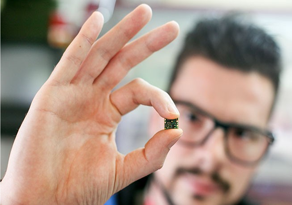
At Adeia, our experts innovate beyond conventional semiconductor technologies, creating advanced solutions that are revolutionizing the design and manufacturing of electronics and shaping the future of the semiconductor industry.
Our hybrid bonding solutions enable chips and wafers to be bonded with ultra-fine pitch 3D electrical interconnects at room temperature without pressure or adhesives.
This patented process uses a modest thermal treatment to create a pristine, all copper interconnect surrounded by inorganic dielectric that delivers high reliability and enhanced thermal performance.
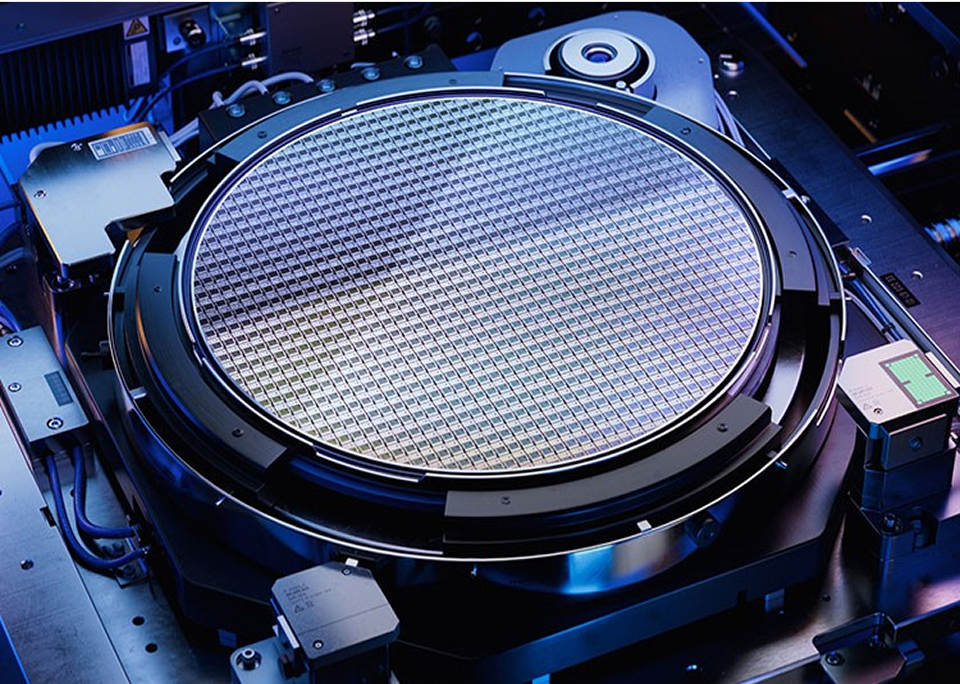
DBI® wafer-to-wafer hybrid bonding is a low temperature technology platform that leverages industry-standard wafer bonding equipment. High-throughput, low-cost 3D interconnects can be realized for your high-volume market applications. The DBI® platform is ideal for applications with the same size die on each wafer, such as image sensors, antenna switches, and 3D NAND memory stacks to enhance manufacturing efficiency, reduce production costs, and improve device performance.
Learn MoreDBI® Ultra is a low-temperature, die-to-wafer and die-to-die hybrid bonding technology platform that enables stacking with any die size, processed on diverse technology nodes, and fabricated on different wafer sizes and materials. DBI® Ultra is ideal for advanced 2.5D, 3D, and 3.5D heterogeneous integration of memory and logic systems that include HBM, CPUs, GPUs, TPUs, or SoCs.
Learn More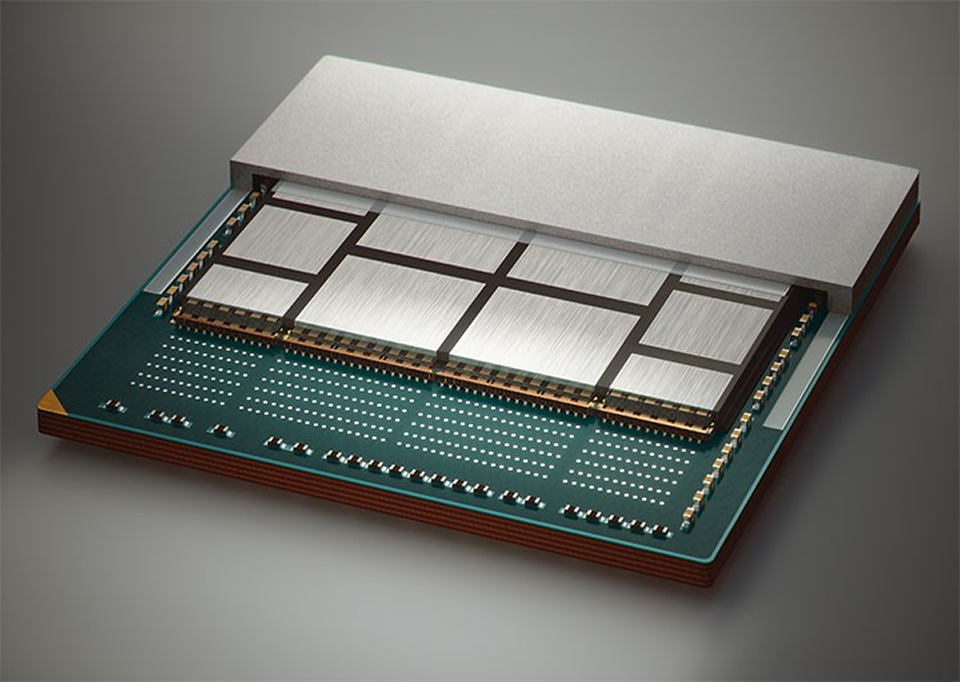
© 2026 Adeia Inc. All Rights Reserved |
Terms & Conditions |
Privacy Policy |
Accessibility