Cookie Preferences

January 22, 2025
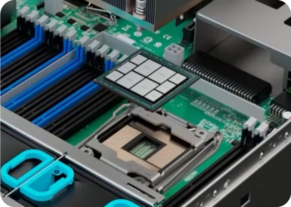
Adeia’s hybrid bonding technology is revolutionizing chip design and manufacturing with ultra-fine pitch, low-inductance, low-capacitance, and low-resistance interconnects. Setting new standards for efficiency and reliability.
Watch VideoMarch 14, 2023
Adeia’s 30 years of semiconductor research and development is enabling innovations in chip scale packaging, delivering smaller, faster, denser interconnects for enhanced data transfer.
Watch Video

November 8, 2022
In this webinar, you’ll learn how hybrid bonding technology enables small-footprint heterogeneous integration while increasing efficiency, performance, and reliability.
Watch VideoOctober 5, 2022
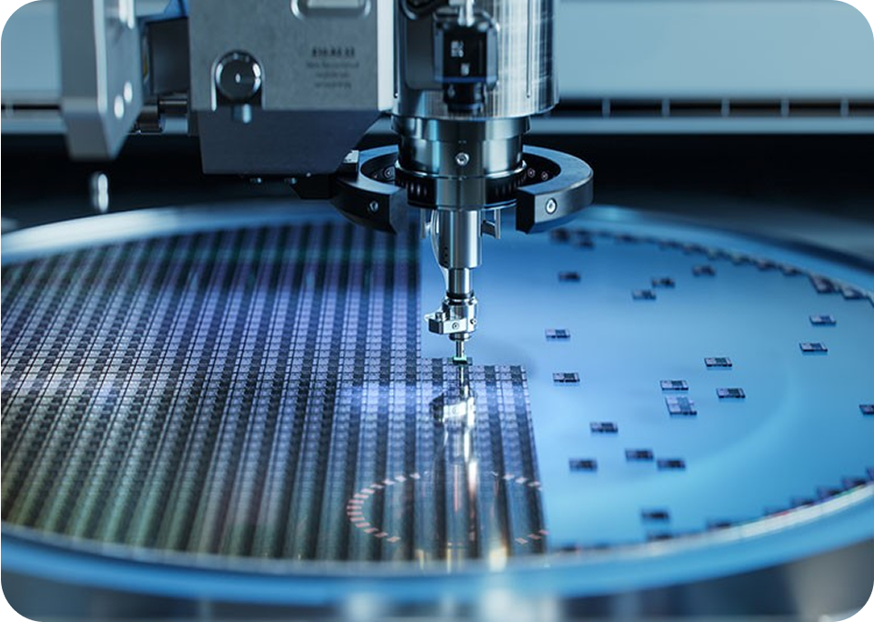
Watch this demonstration of low-temperature wafer-to-wafer hybrid bonding that enables fine pitch 3D electrical interconnects.
Watch Video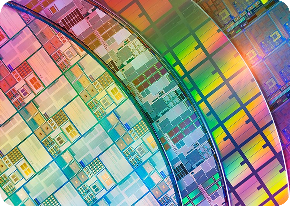
October 5, 2022
See how Adeia’s demonstration of die-to-wafer hybrid bonding eliminates the need for copper pillars and underfill while resulting in dramatically thinner stacks.
Watch VideoOctober 5, 2022
DBI® Ultra hybrid bonding enables high-bandwidth and high-performance computing with 2.5D, 3D, and 3.5D integration of logic and memory applications including HBM, CPU, GPU, FPGA, or SoC.
Watch Video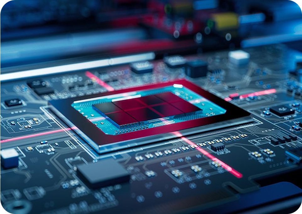
© 2026 Adeia Inc. All Rights Reserved |
Terms & Conditions |
Privacy Policy |
Accessibility