Cookie Preferences

May 14, 2026
Adeia recently joined Roth Capital Partners for another in-depth Tech Talk focused on two of the most important technologies shaping the architecture behind semiconductor applications: hybrid bonding and direct-to-chip cooling.
Hosted by Scott Searle, Communications, AI, IoT, and Edge AI Analyst at Roth Capital Partners, the April 2026 discussion featured Dr. Laura Mirkarimi, SVP of Engineering at Adeia Semiconductor and one of the industry’s leading voices in hybrid bonding, advanced packaging, and thermal management.
The conversation explored how hybrid bonding is accelerating adoption across 3D NAND, HBM DRAM, logic chiplets, hyperscaler infrastructure, and edge AI, while also examining how Rapid Cool™, Adeia’s direct-to-chip cooling technology, could help the industry address escalating power densities in AI systems.
For those who missed the session, here is a recap of the key themes, market implications, and why Adeia believes these technologies are becoming essential building blocks for the AI era.
As AI models grow more complex and data-intensive, semiconductor design is being pushed beyond the practical limits of traditional packaging and monolithic architectures. Designers need more memory bandwidth, lower power consumption, smaller form factors, and better thermal performance — all at once.
That is where hybrid bonding comes in.
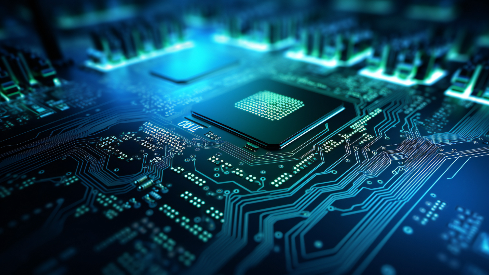
Hybrid bonding is an advanced interconnect technology that creates direct dielectric-to-dielectric and copper-to-copper bonds between two surfaces. Unlike conventional microbump-based approaches, it removes much of the interconnect overhead that limits performance and thermal efficiency.
As Dr. Mirkarimi explained during the Tech Talk, hybrid bonding delivers meaningful advantages because it allows chip to chip connectivity with extremely fine-pitch interconnects with lower parasitics and much better thermal characteristics.
The core benefits include:
In practical terms, that means chips can communicate faster, use less power, and operate more efficiently in the increasingly dense environments required for AI training, inference, and advanced computing.
One of the most important themes from the discussion was that all roads increasingly lead to hybrid bonding.
In 3D NAND, hybrid bonding is already becoming a critical enabler as layer counts continue to rise. During the discussion, Dr. Mirkarimi noted the momentum in the NAND market, including transitions at very high layer counts and public plans by additional manufacturers to adopt hybrid bonding in future generations. The reason is simple: when memory suppliers need to improve performance and power efficiency while maintaining competitiveness, hybrid bonding gives them a compelling path forward.
In HBM DRAM, the driver is especially clear: thermals.
As HBM stacks move higher and AI workloads become more demanding, traditional interconnect technologies create temperature gradients that can force memory throttling. Hybrid bonding reduces thermal resistance across the stack, helping memory operate closer to intended performance levels. While evolving standards may create flexibility for incumbent approaches in the near term, Adeia’s view is that hybrid-bonded HBM remains a critical long-term direction because of its electrical and thermal advantages.
In logic and chiplet architectures, hybrid bonding is equally transformative. AI processors are getting larger, more complex, and more expensive to manufacture monolithically. With chiplet architectures, designers can disaggregate functions like logic, SRAM, I/O, and memory into separate dies, optimize each for cost and performance, and then reconnect them with extremely efficient interfaces.
This improves both yield and cost structure while giving architects more flexibility. As highlighted in the Tech Talk, companies such as AMD have already demonstrated the value of this approach, and the broader market is moving in the same direction. As chiplet architecture matures, hybrid bonding is expected to become an increasingly important way to unlock performance enhancements with greater manufacturing flexibility.
A major focus of the discussion was Adeia’s long-standing leadership in hybrid bonding.
Adeia’s position in the market is built on years of development, including the foundation established through the Ziptronix acquisition and the continued work of Adeia’s engineering teams to make hybrid bonding manufacturable in real-world semiconductor environments.
As Dr. Mirkarimi described, Adeia’s portfolio extends well beyond the basic bond structure itself. It includes innovations across:
This matters because hybrid bonding is not just a single invention. It is an entire manufacturing and ecosystem challenge. To scale in high-volume manufacturing, companies need not only foundational IP, but also practical process knowledge, inspection strategies, metrology, and repeatable integration steps.
That combination of IP depth and real process understanding is one reason Adeia believes its technology has become so relevant as hybrid bonding adoption expands across the industry.
The second major theme of the Tech Talk was Adeia’s technology Rapid Cool™, which is, direct-to-chip cooling.
As AI accelerators become more powerful, chip power densities are rising sharply. Traditional cooling solutions can only go so far, especially as the industry tries to avoid large infrastructure changes or excessive system complexity.
The RapidCool™ solution is designed to address that challenge by dramatically reducing thermal resistance at the chip interface. As presented in the discussion, Adeia’s approach removes the conventional thermal interface material (TIM) bottleneck and replaces it with a silicon-based cold plate concept that can significantly improve cooling performance.
According to Adeia’s internal development work discussed during the Tech Talk, the company has observed:
That last point is especially important. Adeia is not trying to force a complete architectural reset. Instead, the goal is to provide a solution that can integrate into the existing ecosystem more naturally, which may help lower barriers to adoption and extend the current infrastructure in datacenters for several generations of performance upgrades.
While hybrid bonding is already well into commercialization, the RapidCool™ technology is earlier in its lifecycle. But the market need is becoming easier to understand.
If hybrid bonding enables more chips to be stacked and placed closer together, the resulting modules will need even better thermal management. In that sense, hybrid bonding and direct-to-chip cooling are complementary technologies.
Adeia’s view, as discussed in the Tech Talk, is that the eventual trigger for adoption will come when the economics of cooling, performance, and total energy cost make today’s approaches less viable. The exact timing remains to be seen, but the trajectory is clear: AI data centers and advanced compute systems will need more effective and more scalable cooling solutions.
The April 2026 Roth Tech Talk reinforced a consistent message from Adeia: hybrid bonding is no longer a future concept — it is a foundational technology for the next generation of memory and logic design. And as system power densities keep climbing, direct-to-chip cooling may become just as important to enabling the next wave of AI hardware.
For semiconductor companies, hyperscalers, and ecosystem partners, the takeaway is straightforward. The future of high-performance computing will be shaped not just by transistor scaling, but by advances in interconnect technology, advanced packaging, and thermal management.
Adeia is working at the intersection of all three.
Watch the Tech Talk replay: Register to watch here

Laura Mirkarimi is SVP, Head of Semi Engineering at Adeia Semiconductor, San Jose, California. She earned a PhD in Materials Engineering at Northwestern University and a B.S. in Ceramic Sci. & Eng. from Pennsylvania State University. Dr. Mirkarimi leads the Engineering team at Adeia. Known for her pioneering work in hybrid bonding, she continues to focus on key technologies to enable future generations of electronic products including advanced packaging, metrology and thermal solutions. She holds over 100 patents and 60 technical publications. Prior to joining Adeia, she developed electronic devices including ferroelectric memory, transparent conductors and photonic crystal sensors at Hewlett Packard Laboratories for 12 years. As VP of Electronics Segment Marketing at Zeiss Microscopy, she worked with the R&D and product manufacturing teams to build the product roadmap for x-ray microscopy.
© 2026 Adeia Inc. All Rights Reserved |
Terms & Conditions |
Privacy Policy |
Accessibility